
Hansol IONES ultra-precision coating technology improves yields
and productivity such as stabilizing parts and atmosphere
and extending the life of parts through coating of parts
used in Plasma Chamber during semiconductor and display
Major coating technologies include APS, SPS, DLC, INC, etc.
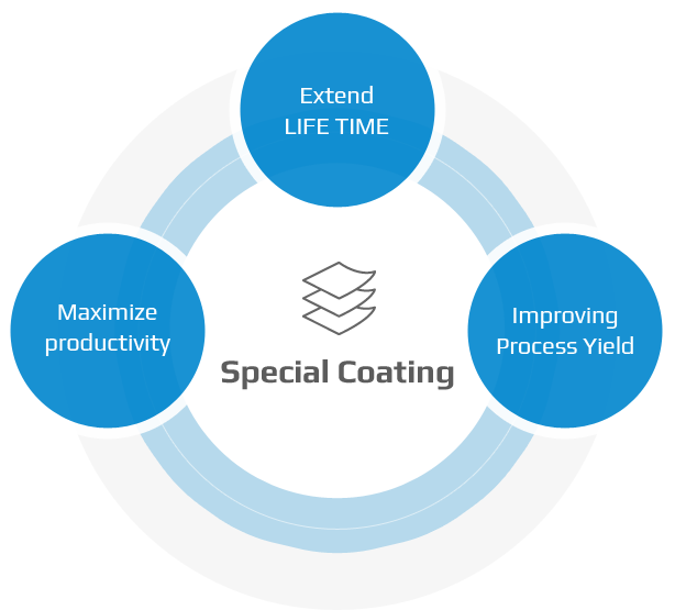
Extend LIFE TIME
Reduce part One-Out and increase durability
Part Life Time Management through Part History Management
Maximize productivity
Reduce Backup Time
Equipment Condition Stable Management
Improving Process Yield
Particle Reduction
Arcing Zero with Special Coating
BELLJAR
-
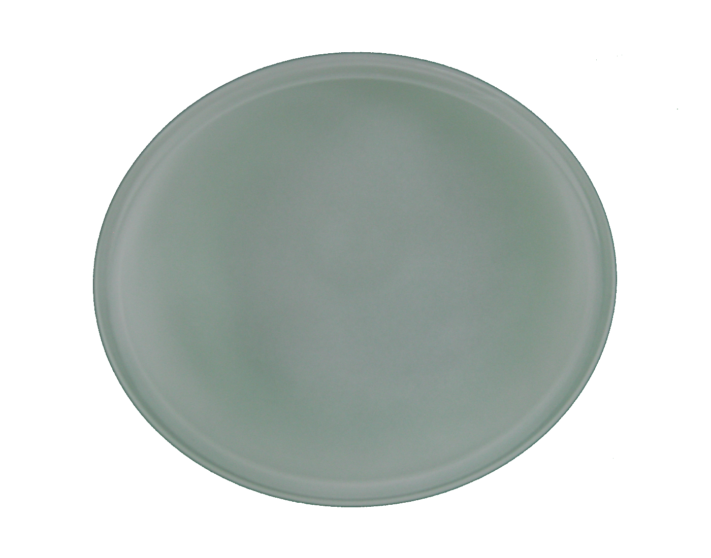
Before coating
-
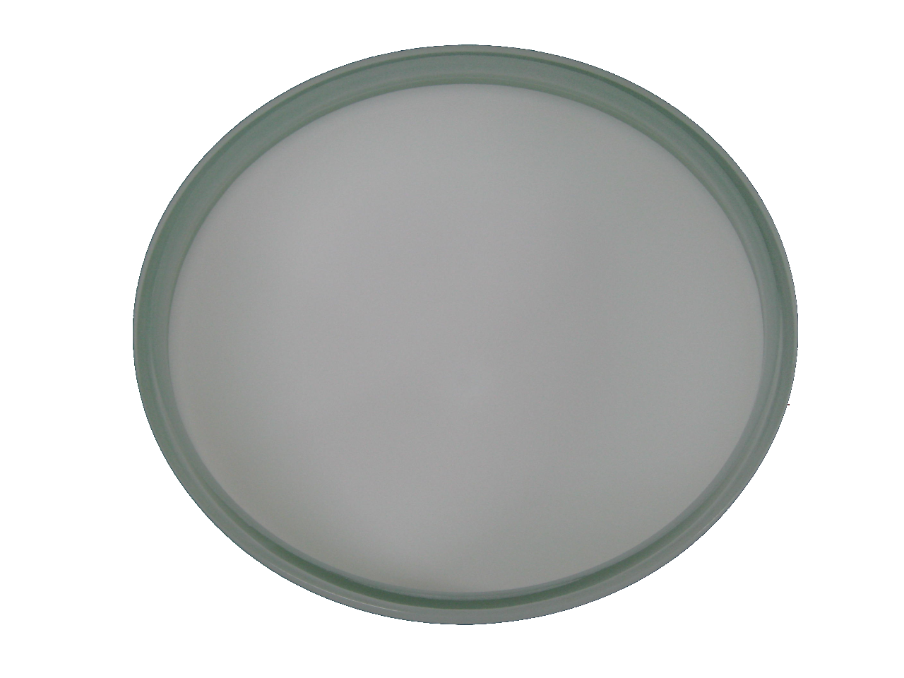
After coating
CERAMIC DOME
-
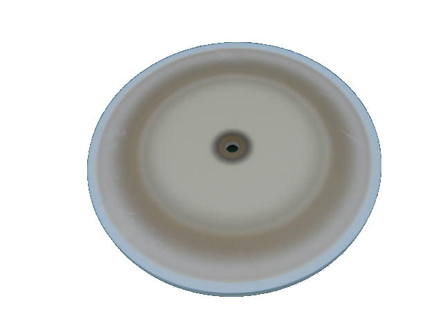
Before coating
-
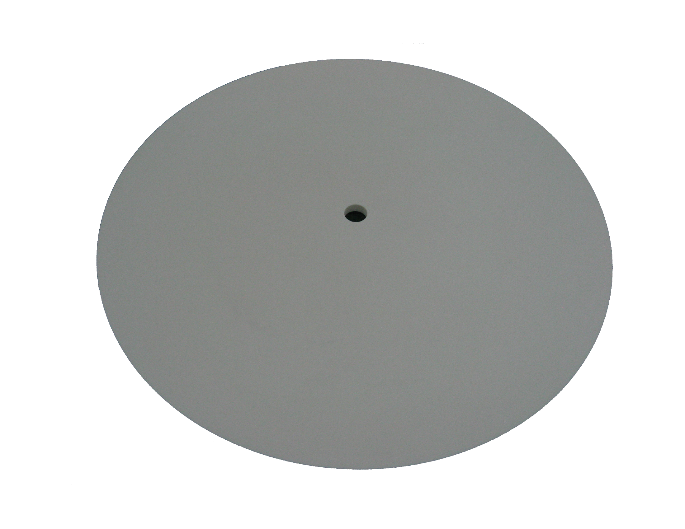
After coating
COVER BELLOWS
-
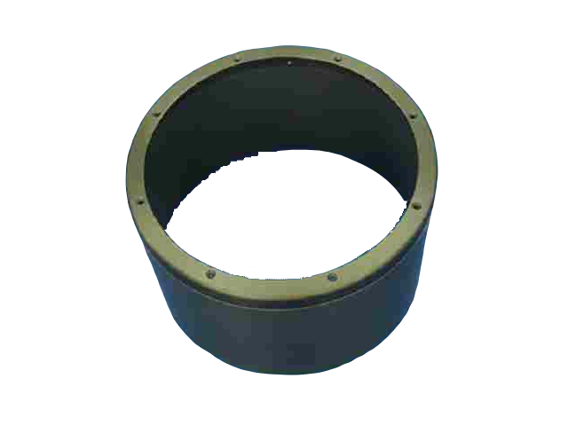
Before coating
-
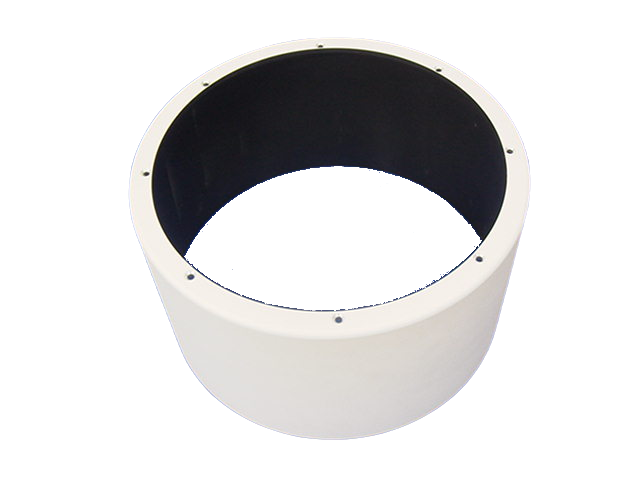
After coating
DEPO SHIELD UPPER
-
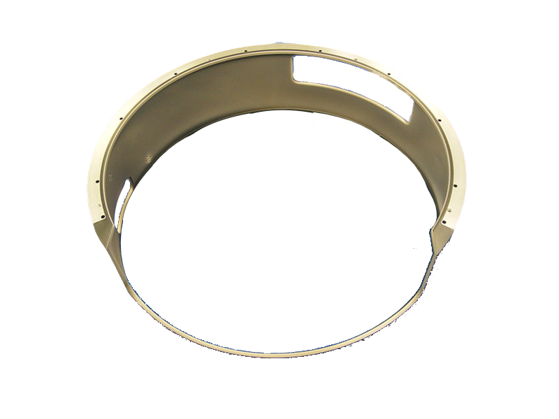
Before coating
-
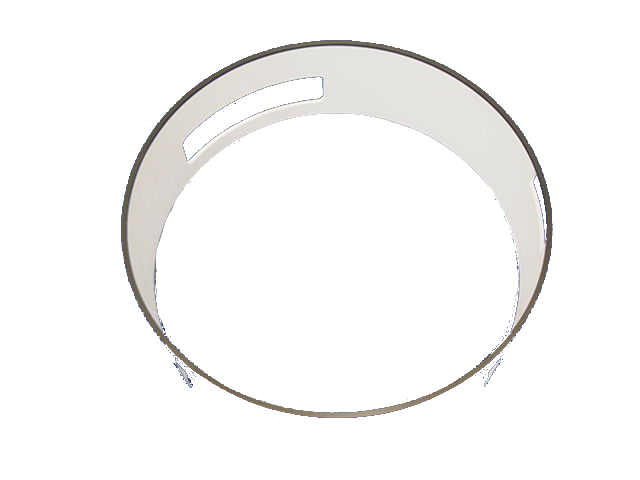
After coating
EPD WINDOW
-
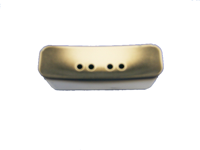
Before coating
-
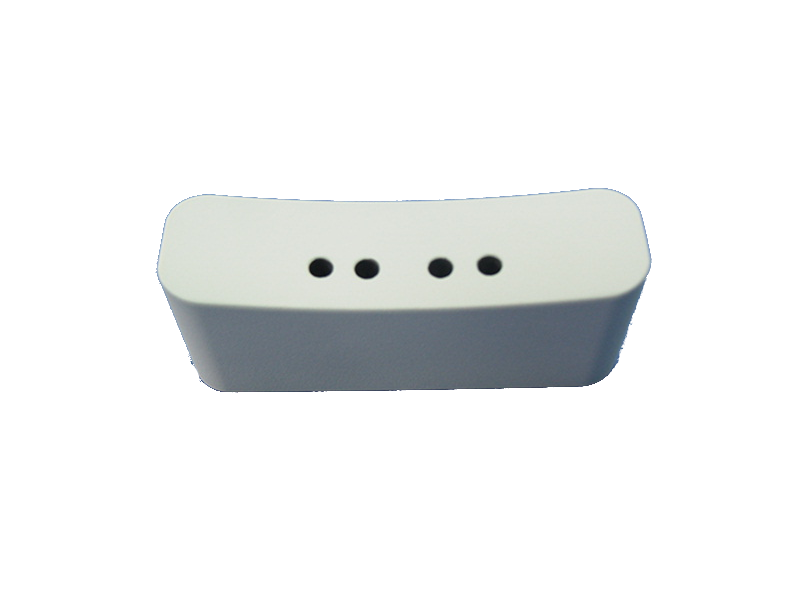
After coating
Coating Technology
Coating Type
| Items | PVD (Physical Vaper Deposition) |
ALD (Atomic Layer Deposition) |
APS (Atmosphere Plasma Spray) |
|---|---|---|---|
| Description | A process in which material is melted under high vacuum using an electron beam, then accelerated and deposited onto a substrate through plasma ionization. | A technology that injects precursors alternately, enabling self-limiting surface reactions for ultra-thin, uniform, and dense films at an atomic scale. | A method where raw materials are melted and sprayed onto substrates using high-temperature plasma in atmospheric conditions. |
| Key Benefits | Achieves high-density, high-hardness thin films to minimize particle generation. | Provides 3D conformal coatings, pinhole-free films, and excellent plasma resistance. | Offers excellent plasma resistance for semiconductor parts, minimizing particle generation and stabilizing processes. |
| Cross section | 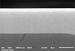 |
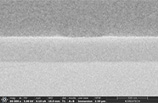 |
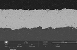 |
| Hardness [Hv] | Y2O3(1100) YAG(1500) Al2O3(1500) |
Y2O3(1100) YAG(1100) Al2O3(1200) |
> 450 |
| Porosity [%] | < 0.01 | < 0.01 | < 1.5 |
| Items | SPS (Suspension Plasma Spray) |
INC (Hansol IONES Nano Coating) |
DLC (Dual Layer Coating) |
|---|---|---|---|
| Description |
A coating technology that disperses fine ceramic powders into a liquid slurry and sprays them using plasma. |
A coating technology that forms a dense coating layer by accelerating ceramic powders at supersonic speeds onto the substrate under low vacuum at room temperature. | A technology that forms a dense INC layer on the surface of APS-coated substrates. |
| Key Benefits | Enhances the mechanical properties of the coating and improves the surface particle condition. | Minimizes surface particle generation. | Improves coating surface density and reduces surface particles. |
| Cross section | 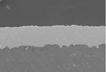 |
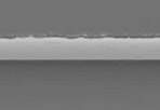 |
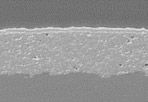 |
| Hardness [Hv] | 450~550 | 300~500 | 300~400 |
| Porosity [%] | < 1.0 | < 0.5 | < 0.5 |
APS Coating Details
| Items | APS (Atmosphere Plasma Spray) |
||||
|---|---|---|---|---|---|
| Y2O3 | YOF | SPC | PRC | PIC | |
| Description | A coating technology that melts and sprays ceramic powders such as Y2O3, Al2O3, YAG using an arc plasma heat source to form a solid coating layer. | ||||
| Key Benefits | Excellent plasma resistance | Reduces back-up time and controls changes over time | Improves coating surface roughness, hardness, and porosity | Enhanced resistance to F and CI ion plasma atmospheres | Reduces particle generation |
| Cross section | 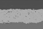 |
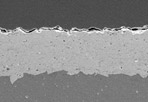 |
 |
 |
 |
| Hardness [Hv] | 400~500 | 350~450 | 450~550 | 450~550 | 500~600 |
| Porosity [%] | < 3.0 | < 3.0 | < 1.5 | < 2.0 | < 3.0 |
Surface Treatment Technology
| Items | Fluorine Surface Treatment | Plasma Cleaning |
|---|---|---|
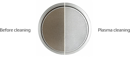
| Description | A technology that applies fluorine plasma treatment to the surfaces of materials such as Y2O3, Al2O3,YAG, anodized layers, Ni, and Al to form a fluorine compound layer. | A technology that utilizes oxygen (O2) and fluorine (F) plasma to remove organic and inorganic contaminants from the surfaces of semiconductor parts, enabling their reuse. |
| Key Applications | Reduction of back-up time for coated parts | Cleaning and recycling of quartz, aluminum, and ceramic parts used in semiconductor processes. |
| Performance | Reduction of surface roughness Surface fluorine atomic percentage: 20–70% |
Removal of surface contaminants (such as carbon and oxides) Extended lifespan through parts recycling Suppression of particle generation |
| Key Benefits | Improving customer productivity by reducing back-up time | Reducing material costs through parts recycling Lowering customer operating expenses and improving productivity |
| Benefits | 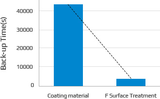 |
 |